E-Paper Calendar V2 Hardware: V1 Validation and V2 Design
This article is migrated from Medium and translated by Gemini pro 2.5.
(Article produced by Gemini 2.5 Pro, with personal revisions.)
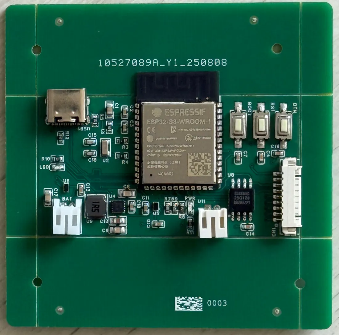
Following the last post where I shared the design philosophy of the e-paper calendar, and after a period of waiting, we finally received the first version of our custom PCB! This article will document the initial verification work we did on this new board and, based on the problems and cost considerations we found in V1, outline the improvement plan for our next version (V2).
V1 Board Verification: Ensuring a Solid Hardware Foundation
The moment I got the board, I was naturally both excited and nervous. To ensure that the subsequent software development could proceed smoothly, we verified each key part of the circuit board according to our plan:
- Power Short-Circuit Test: Before connecting any power, we used a multimeter to carefully check for shorts between the power input, the main power outputs, and the ground line. This step is crucial to avoid any “magic smoke” and ensure there are no fatal hardware errors.
- Power-On Voltage Check: After confirming no shorts, we carefully connected the USB power. We used a multimeter to measure the supply pins of each key IC to see if the voltages were normal (e.g., if the 3.3V LDO output was stable at 3.3V).
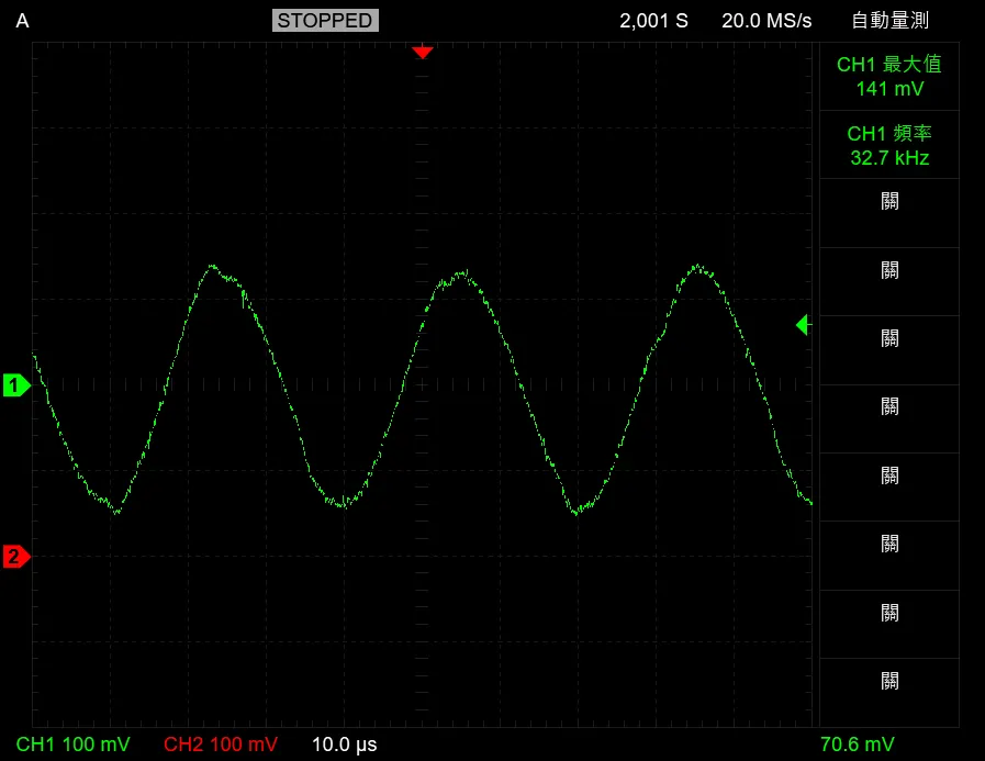
- RTC Crystal Waveform Measurement: We used an oscilloscope to probe the pins of the 32.768kHz external crystal and successfully observed a clean sine wave at the correct frequency. This verified that our RTC clock source was working, which is vital for precise sleep and wakeup.
- USB Flashing Test: We tried flashing the ESP32-S3 directly via the USB-C port. Surprisingly, the flash completed successfully even without holding the BOOT button! This is thanks to the ESP32-S3’s built-in USB-OTG functionality. Nevertheless, considering the device might need to be forced into bootloader mode from Deep Sleep or other special states, we decided to keep the BOOT button in the next version as a hardware-level backup.
- Self-Test Firmware: To more comprehensively validate the hardware, we wrote a simple “Hello World” firmware that included:
- Printing a boot-up log message to the Serial Monitor.
- Blinking the onboard LED.
- Scanning the I2C bus to confirm the BQ25180 power management IC and the MAX17048 fuel gauge IC could be detected.
- Setting the RTC to enter a short sleep and printing a log after waking up.
Overall, the V1 verification process was incredibly smooth, which gives us great confidence for the development ahead!
V2 Circuit Improvement Plan: The Trade-off Between Cost and Battery Life
Building on the V1 verification, we also carefully analyzed the current design and planned the following improvements for the V2 circuit, focusing on cost, power consumption, and usability:
- Power Indicator LED Optimization: We noticed the green power LED on V1 stays brightly lit as long as the board is powered. In actual use, this can be distracting and consumes extra power, which is detrimental to our goal of long battery life. Therefore, in V2, we will remove this always-on power indicator.
- Changing Charging IC to TP4057: To significantly reduce cost, we decided to switch to the more economical TP4057. What is power path management? Simply put, it ensures that when multiple power sources are present (like USB and battery), the system can intelligently select the appropriate source and switch between them smoothly. Since the TP4057 lacks this feature, we will use a P-MOSFET (AO3401A) and a Schottky diode (SS34) to build a simple but effective power path management circuit.
- Keeping the Fuel Gauge IC (MAX17048): We had considered using a simple voltage divider to estimate battery level, but given that the MAX17048 can provide a much more accurate battery percentage (SoC) and voltage, it’s still crucial for user experience and fine-grained low-battery management. We decided to keep this IC in V2.
- ESP32-S3 Soldering Method Adjustment: One of the most expensive parts of V1 was paying the factory for SMT assembly of the ESP32-S3 module. To drastically cut costs, I decided to challenge myself to hand-solder it in V2. But here’s the problem: the ESP32-S3 module has a large ground/thermal pad on the bottom, which usually requires a hot air gun to solder perfectly. Since I only have a regular soldering iron, I discussed solutions with Gemini. The final plan: on the PCB, at the corresponding thermal pad location, I won’t pour copper. Instead, I’ll place several large plated through-holes. This way, during soldering, I can feed solder from the back of the PCB through these holes, allowing my soldering iron to solder the bottom thermal pad to the GND plane. This is a practical trick for handling QFN/LGA packages with only a soldering iron.
- Component Library Optimization: When selecting components, we will also try our best to choose parts from JLCPCB’s “Basic Parts” library to avoid extra “Extended Parts” fees.
V2’s Main Risk: The Screen Driver Circuit
While V2’s goals are cost reduction and higher integration, it also introduces new technical risks. The biggest challenge among them is integrating the e-paper’s driver circuit onto the board for the first time.
To ensure success, I carefully studied Waveshare’s official driver circuit. The V2 schematic and component selection are basically a complete copy of the official design.
However, an e-paper driver circuit (especially the high-voltage Boost circuit) is extremely sensitive to PCB layout. The official module’s layout has its own tricks, and it’s uncertain whether my own layout can achieve the same stability.
This is the highest-risk part of V2. If the Boost circuit is unstable or creates too much interference due to poor layout, the worst-case scenario is that the screen doesn’t light up at all. That would mean the V2 board is a failure. This will be the part I’ll be holding my breath for during the next round of hardware validation.