E-Paper Calendar V2 Hardware: The Story of the First PCB
This article is migrated from Medium and translated by Gemini pro 2.5.
(Article written by Gemini 2.5 Pro, with only minor word adjustments by me.)
When you hit a certain stage of software development, you can sometimes feel a bit fatigued. The repetitive cycle of testing and debugging makes you need a change of scenery. At times like these, shifting your focus from code to a soldering iron and a circuit board is undoubtedly the best medicine.
So, I designed the first version of the PCB for the e-paper calendar project and placed an order with JLCPCB.
This post will share my reasoning for selecting the core components for this first version, some considerations that went into the PCB design, and a frank look at the… surprisingly high cost.
V1 Hardware Philosophy: Function First, Cost Second
For the first version of my custom hardware, my core philosophy was “function verification first.”
I wanted this board to be a “complete package,” something that could validate all my product feature ideas, especially the highest-risk and most central parts: extreme low power and precise power management.
Therefore, I didn’t make many compromises on component selection. The goal was to build a stable and reliable development platform to get the software and user experience right first. Cost optimization would be the mission for the next version, V2.
Core Component Selection and Rationale
Based on the “function first” principle, I chose the following key components:
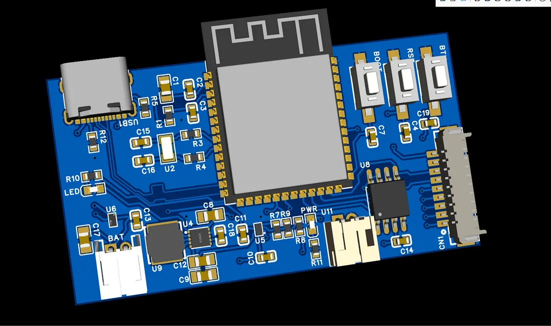
1. Main Controller (MCU): ESP32-S3-WROOM-1
The ESP32-S3 is currently the star of the ESP32 family. It not only has a powerful dual-core processor and ample I/O, but also excellent Deep Sleep performance and native USB OTG. This means it can be flashed and communicated with directly via USB-C, saving an external USB-to-UART chip and simplifying the circuit.
2. The Heart of Precise Timing: 32.768kHz External Crystal
Although the ESP32 has an internal RTC, its built-in RC oscillator suffers from severe temperature drift and has poor timekeeping accuracy. It’s completely unsuitable for applications needing precise, long-term sleep and wakeup. To allow the calendar to wake up at the “second” level after sleeping for an hour or a day, a high-precision 32.768kHz external crystal is indispensable.
3. Storage Space: W25Q128 (16MB SPI Flash)
To support beautiful Mandarin (Chinese) fonts and future additions like images and icons, the ESP32-S3 module’s built-in flash might be tight. Adding an external 16MB SPI Flash allows me to store font files and image resources without worry, and even use it as a buffer for OTA firmware updates.
4. A Robust Power Management System (PMS)
This was the most meticulous and most expensive part of this design. The goal was to achieve safe charging, accurate battery gauging, and high-efficiency power conversion.
- Charging IC (BQ25180): This chip from Texas Instruments (TI) is a highly integrated Power Management Unit (PMU). It not only provides stable and reliable Li-ion battery charging management (with precise I2C control over current, voltage, etc.) but also integrates power path management and an LDO. It’s an “all-in-one” solution that gives a designer great peace of mind.
- Fuel Gauge IC (MAX17048): The question “How much battery is left?” is very poorly answered by simply measuring voltage. The MAX17048 is a dedicated Fuel Gauge IC. It uses Maxim’s proprietary ModelGauge algorithm to accurately calculate the battery’s remaining State of Charge (SoC), which is crucial for improving the user experience.
- Boost-Buck Regulator (TPS63031): A Li-ion battery’s voltage drops from a full 4.2V down to around 3.0V. If you only use an LDO (Low-Dropout) regulator, the ESP32 will stop working stably once the battery voltage drops below 3.3V, wasting battery capacity. The TPS63031 is a Buck-Boost chip that can stably output 3.3V whether the input voltage is higher or lower than 3.3V. It squeezes out every last drop of power from the battery and is the soul of a long-endurance design.
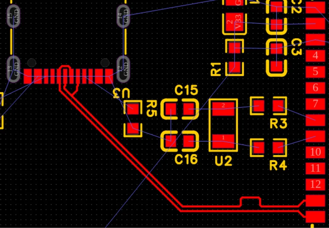
PCB Design Considerations: Why a 4-Layer Board?
For maker projects, 2-layer boards are common because they’re cheap. But this time, I opted for a slightly more expensive 4-layer board for a few key reasons:
- A Solid Ground Plane: This is the most important reason. A 4-layer board allows me to have an almost completely unbroken internal ground copper layer. This provides the shortest possible return path for all signals, significantly improving signal integrity and effectively suppressing EMI (Electromagnetic Interference). This is critical for a board that includes Wi-Fi (RF) and sensitive analog circuits.
- A Dedicated Power Plane: The other internal layer can be dedicated to power. This is like building a highway for all the ICs, ensuring they all get a stable, low-noise power supply, which is far better than routing thick traces on the signal layers.
- Simplified Routing, Smaller Area: With dedicated power and ground planes, the top and bottom layers can be used more freely and densely for signals. This made routing easier when dealing with the ESP32-S3’s BGA/QFN package and allowed the entire PCB to be smaller and more compact.
My 4-Layer Stackup:
I used the most classic stackup:
- L1 — Top Layer: Main signal layer. Most components are placed here. Critical high-speed signals (like USB D+/D-) are routed here.
- L2 — Inner Layer 1: GND Plane. A solid copper pour for ground.
- L3 — Inner Layer 2: Power Plane. I split this layer into two main power planes: one
3.3Vplane for the ESP32 and most components, and one5V (V-usb)plane from the USB-C. This split keeps power paths shorter, cleaner, and helps with routing in dense areas. - L4 — Bottom Layer: Secondary signal layer. Fewer components, used for less critical signal lines.
Key Layout Focus Areas:
- Power Path: Following the “where does the power come from, where does it go” principle, I kept the path from the BQ25180 -> TPS63031 -> ESP32 as short and thick as possible. All bypass capacitors must be placed as close as possible to the IC’s power pins.
- ESP32-S3 Module: Strictly followed the official datasheet’s recommendation for the antenna “Keep-out Area.” No copper, traces, or components were placed on any layer underneath the antenna.
- External Crystal: The 32.768kHz crystal and its two load capacitors must be placed tightly together and as close as possible to the ESP32’s corresponding XTAL pins. The traces must be short and direct, and preferably surrounded by a ground pour, kept far away from any high-speed or frequently switching signals (like SPI or the Boost-Buck’s switching node).
- USB-C Differential Pair: The USB D+ and D- lines required “differential pair” routing—meaning they were kept at equal length, equal spacing, and routed in parallel to ensure 90-ohm impedance matching. This is vital for stable flashing and communication.
The Reality of Cost
With everything ready, I excitedly uploaded my Bill of Materials (BOM) and Gerber files to JLCPCB, ready to enjoy the convenience of SMT assembly. And then I saw the quote:
PCB (5 pieces): $7.00 Welding and Assembly: $134.11
The boards themselves were incredibly cheap, but adding the SMT assembly fee caused the per-unit cost to skyrocket. A closer look at the fee structure reveals where the devil is in the details:
- Setup fee: $25.00
- Stencil: $7.86
- Components: $51.15
- Extended components fee: $36.00
- X-ray inspection: $7.85
- … (Other fees)
Where did it get so expensive?
- Fixed Costs (Setup fee, Stencil): These two are fixed costs you have to pay regardless of quantity. For a small batch, this adds a lot to the per-unit cost.
- Extended Components Fee: This was the biggest extra cost! JLCPCB’s parts library is split into “Basic Parts” and “Extended Parts.” Using basic parts costs nothing extra, but for each type of extended part used, they add a ~$3 fee for manual sourcing and loading. A $36 fee means I had about 12 types of extended parts on my board.
- Components Themselves (Components): The TI and Maxim power management ICs I chose are powerful, but their unit price is relatively high.
- A Necessary Evil (X-ray inspection): Because the ESP32-S3 module is a QFN/LGA package, its solder joints are on the bottom. X-ray inspection is necessary to ensure solder quality, making this fee hard to avoid on the first version.
Although the cost isn’t low, I believe these investments are worthwhile for the first version of a function-verification board. It has laid a solid foundation for the subsequent software development and future cost optimization.