E-Paper Calendar V2 Hardware: Haste Makes Waste
This article is migrated from Medium and translated by Gemini pro 2.5.
(Article written by Gemini 2.5 Pro, with personal supervision.)
This article is to document the validation process for the V2 board, an unexpected debugging journey, and, based on this painful experience, the new plan for the next version, V2.1.
V2 Board Validation Report
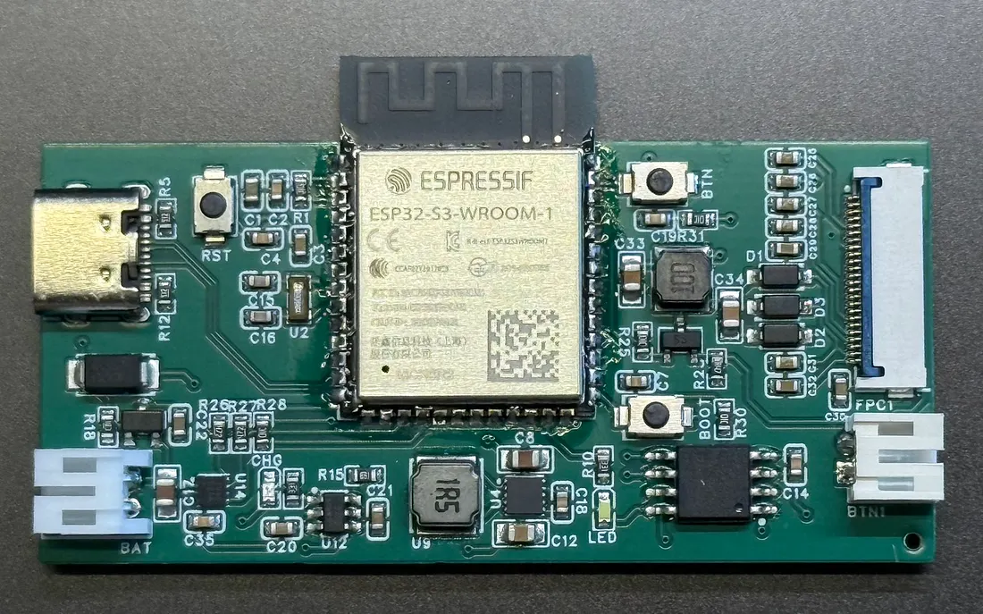
After receiving the board, I followed the plan. I first soldered on the ESP32-S3 module and a few plug-in components, then began the initial verification:
- Basic Validation: Power short-circuit test, and measuring voltages at various points after power-on. Everything went smoothly. The TPS63031 successfully output a stable 3.3V.
- Power Path Management: Confirmed that when both the battery and USB are connected, the battery supply is cut off, and the USB powers the system while charging the battery.
- MCU Flashing: Using the USB-C port,
idf.py flash monitorworked on the first try! The logs printed normally. - I2C Device Scan: After the program ran, it successfully found the address of the MAX17048 fuel gauge IC on the I2C bus.
- RTC: Although my measurement showed an error of about one second, it’s likely not a major issue.
Up to this point, everything was perfect. Next, I started testing another important peripheral: the external SPI Flash (W25Q128).
The SPI Interlude: A Scare from AI
I asked gemini-cli to write me a test snippet to read the JEDEC ID of the W25Q128. After flashing, it just wouldn’t read. Even worse, when I told it my hardware pin connections, it replied: “Your hardware is wired incorrectly. These are reserved pins on the ESP32 and cannot be used for SPI!”
My heart sank when I saw that. Because those SPI lines are shared with the e-paper display, if those pins were truly unusable, not only would the Flash be unreadable, but the screen wouldn’t light up either. The entire board would be a brick.
I immediately went to the electronics store, bought some thin wire and tools, and prepared to perform surgery (bodge wiring) on the board. Just as I was confirming which pins to rewire to, I half-doubtfully opened the Gemini web interface, fed it the ESP32-S3 datasheet, and asked it to double-check. This time, it gave me a completely different answer: “The pins you selected are safe, general-purpose GPIOs and are perfectly fine for SPI.”
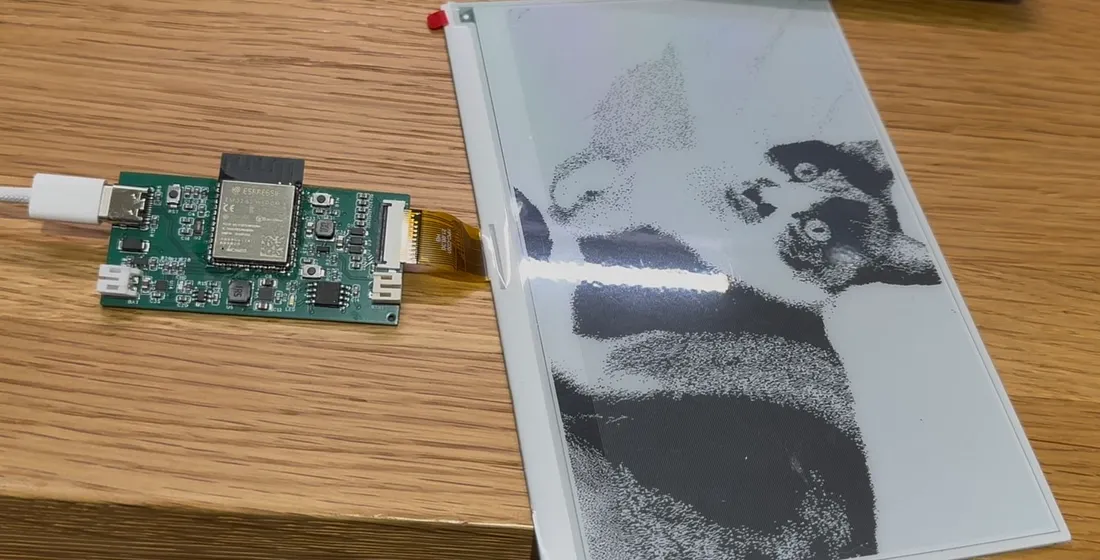
I breathed a sigh of relief. I went back and closely inspected the code gemini-cli had given me, only to find a simple parameter misconfiguration in the spi_transaction_t struct. After a small tweak, the W25Q128’s ID was read successfully! Later, the screen also refreshed without issue. The lesson here: AI writes code really fast, but you still have to check its work. It makes mistakes, too!
At this point, the two riskiest new features of V2—the custom-designed power path management and the integrated screen driver circuit—had both passed their initial validation!
The Deep-Water Challenge: Quiescent Current
With the core functions validated, I began testing the other critical metric: sleep quiescent current. I let the RTC sleep for one minute and measured with a stopwatch. I found the time error was about one second, which surprised me a bit, but it could be measurement error and is probably harmless.
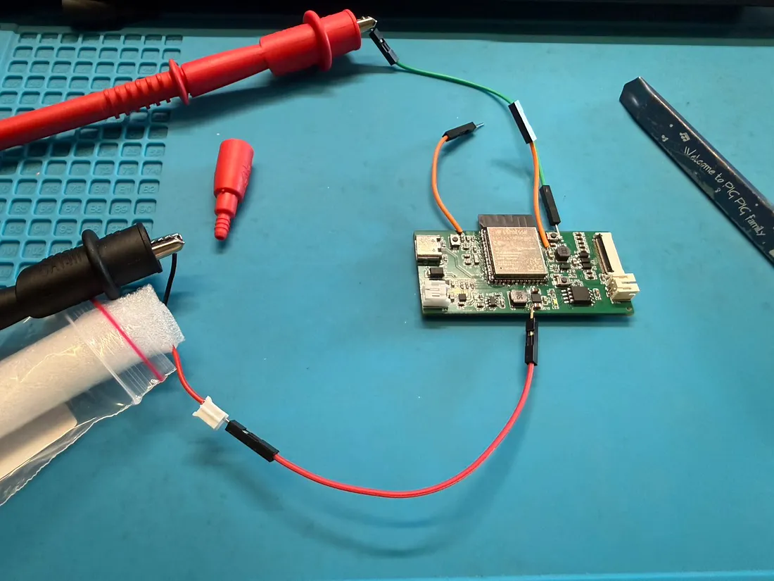
But when I connected my multimeter in series with the battery and put all the ICs into sleep mode, the measured current was… a whopping 5.4mA!
I was shocked. What does this number mean? I asked Gemini to estimate the battery life using this data and an 800mAh battery. It also said this was several orders of magnitude higher than the expected micro-amp (µA) level. At this rate, it would only last a few days, completely defeating the goal of long battery life.
The debugging journey officially began. I used the “process of elimination” method:
- Suspect the screen driver circuit: I cut its power supply. The current did not drop.
- Suspect the ESP32’s incomplete sleep: I held down the RESET button to force the ESP32 chip off. The current still didn’t drop.
- Suspect the power path circuit: I used a wire to bypass it, connecting the battery directly to the TPS63031’s input. The current still didn’t drop.
The clues were getting clearer. There was only one culprit left: the TPS63031 regulator itself. I cut off all of its output loads, letting it run with no load. It alone was consuming nearly 5mA.
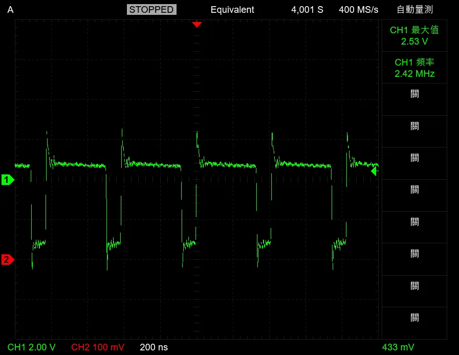
But why? I went back and carefully re-read the datasheet, cross-referencing it with my design. First, the layout. I had previously asked Gemini to read the datasheet and summarize the wiring, but in the end, I still had to read it myself. The reference circuit didn’t quite match—my input/output capacitors were a bit off, and the recommended layout was to widen the power and inductor traces. But these points shouldn’t cause a discrepancy of several hundred times, right? I also measured the waveform with my oscilloscope. Aside from some overshoot during inductor switching, the input and output were relatively stable.
I scoured the datasheet a few more times and finally found the key in a corner: the TPS63031’s Power-Save Mode requires the PS/SYNC pin to be pulled LOW to be enabled!
This seemed to be the main issue. It must enter power-save mode to have a chance of reaching µA-level quiescent current. But this pin was routed very tightly on my board; I had no way to modify it. If I wanted to cut the trace, I’d have to remove the IC. But this IC is tiny and its package is only suitable for hot air removal, which I don’t have.
Although I couldn’t verify the power-save mode, I’m about 70% sure this is the root cause. So, I decided to fix it in the next board revision and turn my attention back to the 300µA current on the load side (this was measured by cutting the TPS63031’s output and measuring the load separately).
300µA is still a bit high. While the estimated battery life is around three months, that doesn’t leave much margin. The actual power consumption will certainly be higher, and in the end, it would likely be less than three months.
(…skipping the tedious debugging process of cutting traces one by one…)
Long story short: The culprit for this 300µA leak was floating SPI bus leakage between the sleeping W25Q128 chip and the ESP32.
- When the W25Q128 was not in sleep mode, the load consumption was ~
900µA. - When the W25Q128 entered sleep mode, the load consumption dropped to ~
300µA. - But if I completely cut the power to the W25Q128, the system’s sleep current successfully dropped to the ideal value of
10µA!
It felt like I had finally reached the end!
V2.1 Redesign: The Quest for Ultra-Low Power
Based on this painful experience, the direction for the next version (which I’m calling V2.1) is crystal clear:
- Fix the TPS63031 Circuit: Strictly follow the datasheet’s layout guidelines and tie the
PS/SYNCpin directly to ground, forcing power-save mode. In theory, this is a light-load circuit, so it shouldn’t affect functionality, but since I couldn’t verify it, I’m still a bit nervous. - Design a Load Power Switch: To completely solve the leakage from peripheral components during sleep, I will add a GPIO-controlled MOSFET power switch. This switch will cut power to all peripherals (Flash, fuel gauge, screen driver) except the ESP32 itself. Before the ESP32 enters deep sleep, it will first use this switch to completely cut power to everything else.
I hope that in the V2.1 board, I will finally see a sleep current in the tens of micro-amps (µA). That would be an ideal milestone for the circuit design.
A Small Reflection
Looking back, the power consumption problems I encountered could have been discovered on the V1 board through more careful hardware and software validation, and then fixed all at once in the V2 version.
All I can say is that “haste” is truly the greatest enemy of development. Because I was in a hurry to see the fully-featured version, I skipped the most thorough power validation for each component, ultimately costing me another round of prototyping time and money for the V2.1 board.
It’s a lesson learned the hard way: next time, I’ll be more patient and finish all planned verification steps before spinning the next revision.
Conclusion
Validating the V2 board was full of challenges, but also full of rewards. We successfully reduced the cost, validated the core functions, and, most importantly, found the root cause of the power consumption issues. Wish me luck, and I’ll see you with V2.1!